.png?width=152&height=65&name=a%20ZEON%20company%20(3).png "a ZEON company (3)")
-1.png?width=152&height=65&name=a%20ZEON%20company%20(4)-1.png "Edge")
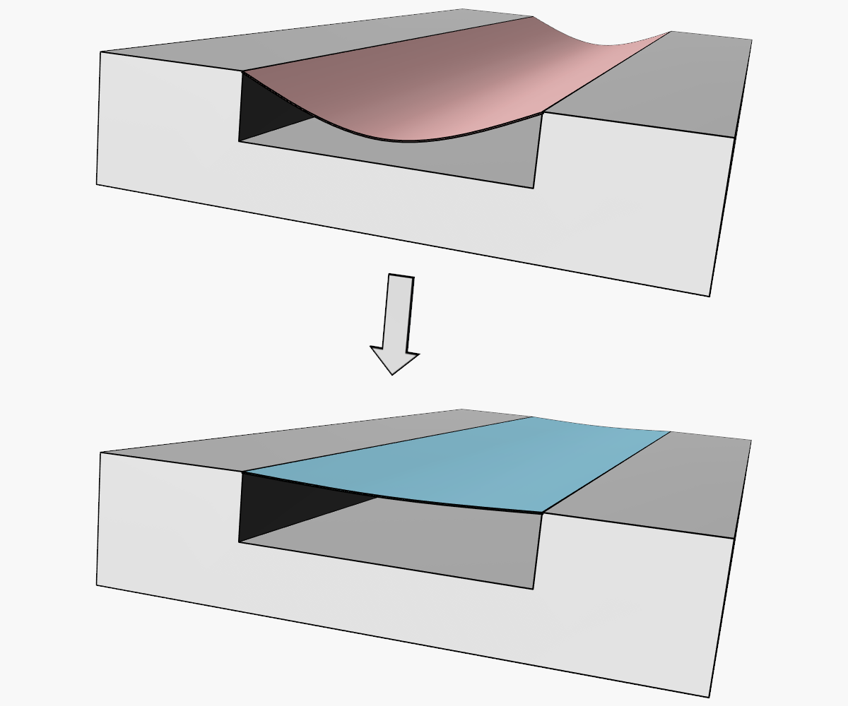
Open geometries are an inherent characteristic of the embossing process. In the fabrication of microfluidic devices, embossing is often used to pattern open-faced, recessed microfluidic pathways on the surface of a polymer substrate. While a subset of microfluidic devices, such as open capillary systems, are designed to operate in an open configuration, most microfluidic applications require the channels to be enclosed on all sides. For example, the simple microfluidic device shown in Figure 1 has channels that are that only partially defined by the embossed substrate and require an additional lidding step to seal the device.
.webp?width=768&height=505&name=Figure%201%20(1).webp)
Figure 1 – An example embossed microfluidic device. The device on the left illustrates an open channel geometry, while the device on the right shows the addition of material that closes channels while still allowing access to inlets and outlets.
Generally, a lid serves three purposes[1]:
- It fully defines the boundaries of the channels.
- It seals the enclosed volume to allow for fluid flow.
- It facilitates selective access to parts of the device, such as inlets and outlets.
There are a few common techniques for sealing microfluidic devices made from thermoplastic. The suitability of each approach for a given application will depend on factors including substrate material, critical dimensions, intended operating conditions (temperature and fluid pressure) and the chemical sensitivity of the assay.
Direct Bonding and Indirect Bonding
Sealing techniques fall into two categories: direct bonding, in which two components are bonded through alteration of the polymer’s surface characteristics, and indirect bonding, in which an intermediate layer adheres the two surfaces[2]. The advantages and drawbacks of each bonding method depend on the specific application and the polymer material of the embossed device. The compatibility of different polymers with each bonding method is summarized in Table 1.
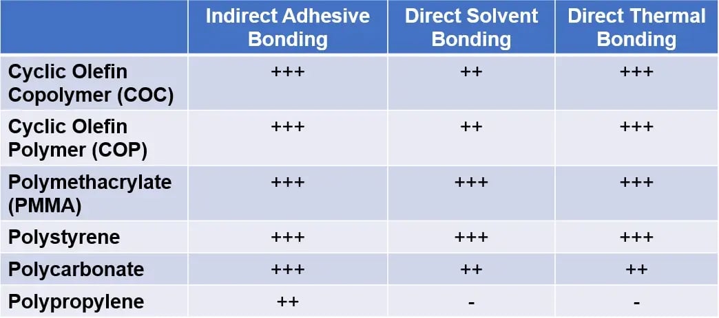
Table 1 – Suitability of bonding method for common polymer substrates: Highly suitable (+++) to non-applicable (-).
Adhesive Bonding
There are two types of indirect adhesive bonding: pressure sensitive and structural. Pressure sensitive adhesives (PSA) are engineered tapes that feature a carrier film and an adhesive coating that is activated by application of uniform pressure. Structural adhesives are liquid based epoxies or adhesives that are activated by chemical processes; for instance, UV- activated adhesives.
Perhaps most suited for rapid-prototyping and disposable devices[3], PSA films have a thin adhesive coating on one side of a plastic carrier film. Lamination of such a material to seal a microfluidic device is often straightforward, typically done at room temperature, by hand or with the aid of a laminator machine.
Microfluidic devices lidded with PSA film are desirable for their ease of fabrication. However, interior channels are often exposed to the adhesives present on the tape. There are several commercially available PSA tapes coated with adhesives that feature low leachables, minimal outgassing, and low autofluorescence — for example, 3M 9795R or ARseal™ 90697. Recent studies on PSA used for lidding have shown functional biocompatibility of specific types of PSAs that make it feasible for organ-on-a-chip devices[4].
In practice, PSA film lamination has limitations specific to the geometry of the microfluidic device. The unsupported region of the lamination film, over channels or other features, can deform inward. The degree of deformation is dependent on several variables, including the amount of force supplied during the lamination process. However, a more structurally robust PSA that limits deformation during lamination can be used[5].
Solvent Bonding
Solvent bonding is a direct bonding method, where the surface of the two polymeric layers are softened with solvents and pressed together. By applying specific solvents to the material surfaces, the polymer-chains gain a degree of mobility and the ability to form new bonds as the solvent evaporates. This method requires specific knowledge of polymer-solvent solubility and may require increased temperatures in order to reach required solubility for creation of bonds[6]. This technique can lead to very strong bonds, as compared to thermal bonding[7], but process parameters, such as excessive solvent exposure time, can lead to deformation or obstruction of the channels[6]. Finally, solvent bonding may be problematic for some applications as residual solvent may be present in the device that can have adverse effects on sensitive chemical assays.
Thermal Bonding
Like solvent bonding, thermal diffusion bonding relies on the interdiffusion of polymer chains at the interface between polymer layers. Instead of introducing a solvent, polymer chains are mobilized by heating the layers to, or near, the glass transition temperature, the point at which the polymer-chains gain sufficient thermal energy to diffuse and form new chain-to-chain bonds upon cooling. In addition to temperature, bonding pressure and hold-time affect the strength of the diffusion bond. Above the glass transition temperature, the material properties of the polymer change, resulting in a marked decrease in stiffness[8]. Bonding the device at the glass transition temperature may have undesirable effects, such as deformation of channel geometries[7]. Therefore, the temperature used to thermally bond the lid to the device is typically lower than the glass transition temperature[9] and should be optimized experimentally for each polymer and application.
Bonding duration and channel width both affect the degree of channel distortion during thermal bonding, as illustrated in Figure 2. Using a laser confocal microscope to image through a lidded device, height profiles of the top and bottom surfaces of a bonded microfluidic channel were mapped and compared to the initial unbonded geometry. A cross section of the height profile shows that both the top and bottom surfaces of the bonded device have crept into the channel under pressure, reducing the height of an initially 50µm tall channel. The reduction in channel height for designs with three different channel widths and two different bonding times are shown in the bar graph in figure 2c). Excessive bonding temperature, time, and pressure may lead to lid sagging and should be dialed back to a point where feature deformation is minimized while still achieving the target bond strength.
.webp?width=975&height=483&name=Figure%202%20(1).webp) Figure 2 – a) 3D height profile of a thermally bonded microfluidic T-junction. b) Cross sectional height profile showing top and bottom surface of the channel. c) Reduction in channel height due to lid sagging for 3 different channel widths and two different bonding durations. These acrylic parts were bonded at 100°C under a pressure of 2MPa.
Figure 2 – a) 3D height profile of a thermally bonded microfluidic T-junction. b) Cross sectional height profile showing top and bottom surface of the channel. c) Reduction in channel height due to lid sagging for 3 different channel widths and two different bonding durations. These acrylic parts were bonded at 100°C under a pressure of 2MPa.
Surface Activation
In addition to the methods of sealing microfluidic devices listed above, device lidding can also be facilitated by surface activation, in which the surfaces to be bonded are exposed to chemically altering process such as oxygen plasma, UV-ozone, or silane modification. Generally, these processes do not penetrate the material, but only activate the exposed surface of the polymer, introducing functional groups. For instance, PMMA exposure to oxygen plasma leads to the temporary creation of reactive oxygen-containing groups[10]. These reactive groups allow for the creation of a strong chemical bond when two activated surfaces are brought together. Surface activation can be combined with thermal or solvent bonding to significantly increase the overall bond strength[3].
Sealing an embossed component is a critical step in realizing a fully functional microfluidic device. As discussed above, there are several factors to consider when selecting the right bonding technique for your application. As such, this step should be taken into consideration early in the process of designing a microfluidic device and selecting its materials. Edge embossing, a custom embossing company, offers post-processing services including packaging and lidding of the final microfluidic device.
References:
[2] Tsao, Chia-Wen, and Don L. DeVoe. “Bonding of thermoplastic polymer microfluidics.” Microfluidics and Nanofluidics 6.1 (2009): 1-16.
[3] Fiorini, Gina S., and Daniel T. Chiu. “Disposable microfluidic devices: fabrication, function, and application.” BioTechniques 38.3 (2005): 429-446.
[4] Kratz, S. R. A., et al. “Characterization of four functional biocompatible pressure-sensitive adhesives for rapid prototyping of cell-based lab-on-a-chip and organ-on-a-chip systems.” Scientific Reports 9.1 (2019): 9287.
[5] Goh, C. S., et al. “Adhesive bonding of polymeric microfluidic devices.” 2009 11th Electronics Packaging Technology Conference. IEEE, 2009
[6] Ng, S. H., et al. “Thermally activated solvent bonding of polymers” Microsystem Technologies 14.6 (2008):753-759
[7] Fiorini, Gina S., and Daniel T. Chiu. “Disposable microfluidic devices: fabrication, function, and application.” BioTechniques 38.3 (2005): 429-446.
[8] Kratz, S. R. A., et al. “Characterization of four functional biocompatible pressure-sensitive adhesives for rapid prototyping of cell-based lab-on-a-chip and organ-on-a-chip systems.” Scientific Reports 9.1 (2019): 9287.
[9] Abgrall, P., et al. “Fabrication of planar nanofluidic channels in a thermoplastic by hot-embossing and thermal bonding” Lab on a Chip 7.4 (2007):520-522
[10] Vesel, A. and Mozetic, M. “Surface modification and ageing of PMMA polymer by oxygen plasma treatment” Vacuum 8.6 (2012): 634-637
[11] Yin, Z. et al. “Fabrication of two dimensional polyethylene terephthalate nanofluidic chip using hot embossing and thermal bonding technique” Biomicrofluidics 8.6 (2014)

EdgeBond: Thermoplastic Bonding for Microfluidics with Minimal Feature Distortion and Lid Sagging
Next-generation microwell and nanowell arrays for single-cell applications
.png?width=600&height=188&name=edge%20forward%20(1).png)